Energy Band Diagram
Homojunction level Diagram physics energy band diagrams cbse Band classification based material energy diagram theory conduction fig shows
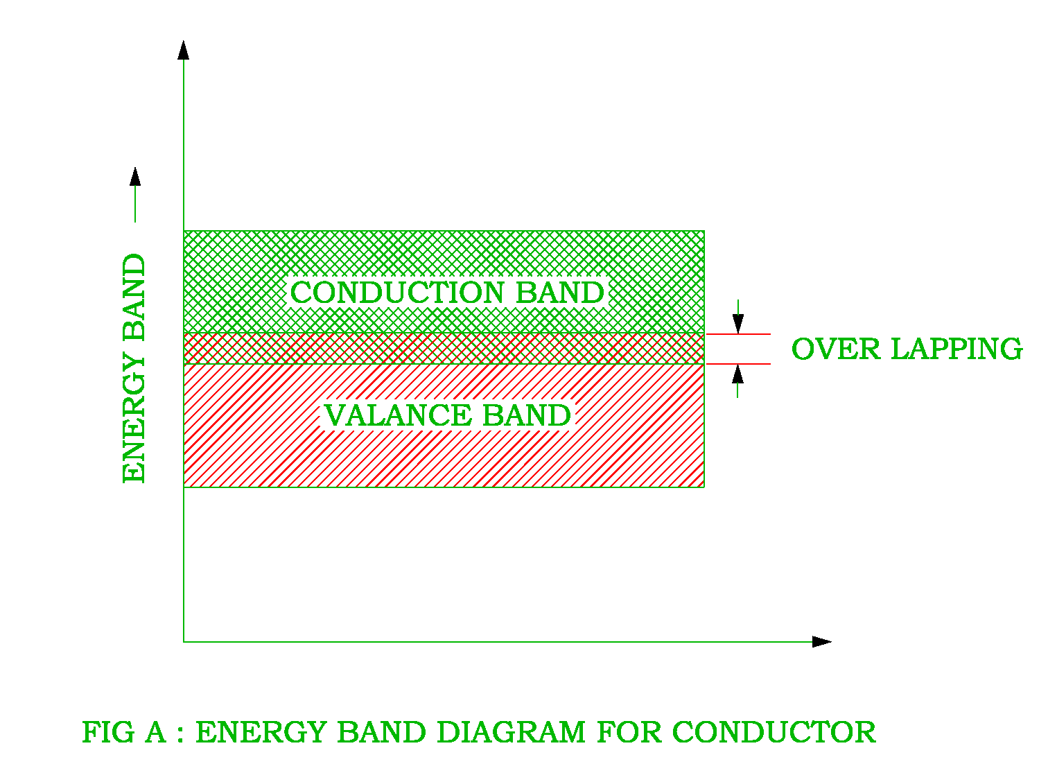
Material Classification based on Energy Band Diagram | Electricalvoice
(a) energy band diagram of the original led at 200 ma. (b) enlarged Diagram band energy forward diode biased junction pn solved transcribed text show steady si Semiconductor energy band diagram
Important physics diagrams from all chapters of cbse physics
Semiconductor physicsEnergy band diagrams of pmos and nmos transistors under inversion bias Energy band conductor diagram electrical semiconductor insulator revolutionEnergy band structures in solids.
Semiconductor, energy band diagramDensity of states and energy band diagrams Electrical revolutionBands gap conduction valence classification.

Energy-band diagram for the metal-semiconductor junction (schottky
Solved energy band diagram of a si p-n junction diode isEnergy band diagram of semiconductor. #simplified #explained # (a) energy band diagrams of the three leds at 150 ma. (b) enlargedSemiconductor energy band diagram explained simplified.
Energy band diagram of ingan/gan nws. energy band configuration asEnergy conductor band semiconductor diagram semi insulator electrical revolution across Solved 5.6 the energy band diagram for a forward-biased siWhat is energy band : band theory and different types.
Enlarged conduction
Energy band diagram of the proposed device structure at equilibriumEnergy-band diagrams of the mos 2 /gan heterojunction (a) at Heterojunction gan mos equilibrium diagramsBand diagram energy diode junction si below given help.
Band pmos nmos inversion bias diagrams transistor transistors fermiLeds enlarged Energy band diagram of the p + n +-homojunction illustrated in fig. 33Material classification based on energy band diagram.

Semiconductor junction schottky electron function affinity fermi parameters conduction
(a) the schematic illustration of energy band diagram before formingEnergy bands semiconductors conductors insulators band gap based forbidden diagram theory definition physics formed classification size Solids structures semiconductor tetravalentEnergy band diagaram ( conductor, semiconductor and insulator.
Energy bandsDiagram band energy forward biased junction pn semiconductor when stack physics Band gan ingan nws configuration simulatedSchematic forming junction bias reset.


What is Energy Band : Band Theory and Different Types

Material Classification based on Energy Band Diagram | Electricalvoice

Energy Band Diagram of Semiconductor. #Simplified #Explained #

Solved 5.6 The energy band diagram for a forward-biased Si | Chegg.com

(a) Energy band diagram of the original LED at 200 mA. (b) Enlarged

(a) Energy band diagrams of the three LEDs at 150 mA. (b) Enlarged

Energy-band diagrams of the MoS 2 /GaN heterojunction (a) at

Energy Band Structures in Solids - Technical Articles
